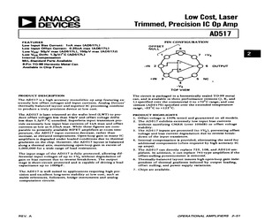
mputation circuits. Low Cost, Laser Trimmed, Precision IC Op Amp The circuit is packaged in a hermetically sealed TO-99 metal can, and is available in three performance versions (J, K, and L) specified over the commercial 0 to +70C range; and one version (AD517S) specified over the full military temperature range, -55C to +125C. The AD517S is also available with full processing to the requirements of MIL-STD-883, Level B. PRODUCT HIGHLIGHTS 1. Offset voltage is 100% tested and guaranteed on all models. Testing is performed using a controlled-temperature drift bath following a 5 minute warm-up period. 2. The AD517 exhibits extremely low input bias currents without sacrificing CMRR (over 100dB) or offset voltage stability. 3. The AD517 inputs are protected (to tVg), preventing offset voltage and bias current degradation due to reverse break- down of the input transistors. 4, Internal compensation is provided, eliminating the need for additional components (often required by high accura
 6 Pages, 428 KB, Scan
, followers, bridge instruments and analog computation circuits. The circuit is packaged in a hermetically sealed TO-99 metal can, and is available in three performance versions (J, K, and L) specified over the commercial 0 to +70C range; and one version (AD517S) specified over the full military temperature range, -55C to +125C. The AD517S is also available with full processing to the requirements of MIL-STD-883A, Level B. PRODUCT HIGHLIGHTS 1. Offset voltage is 100% tested and guaranteed on all models. Testing is performed using a controlled-temperature drift bath following a 5 minute warm-up period. 2. The AD517 exhibits extremely low input bias currents without sacrificing CMRR (over 100dB) or offset voltage stability. 3. The AD517 inputs are protected (to tVg), preventing offset voltage and bias current degradation due to reverse break- down of the input transistors. 4. Internal compensation is provided, eliminating the need for additional components (often required by high accur
 6 Pages, 452 KB, Scan
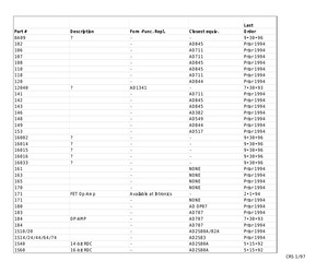
S 1/97 AD395TD AD396SD AD396SD/883B AD396TD AD396TD/883B AD420AN AD420AR AD501 AD501 AD5010/6020 AD502 AD503JH AD503KH AD504 AD505 AD506JH AD506SH/883B AD507 AD508 AD509 AD510LH AD511 AD512 AD513 AD514 AD515 AD515AJH/+ AD515AKH/+ AD516 AD517KH/+ AD517LH/+ AD517SH AD518 AD520 AD5201 AD5202 AD5204 AD5205 Quad 12-bit DAC Quad DAC Quad DAC Quad DAC Quad DAC 16-bit Serial 4-20mA DAC 16-bit Serial 4-20mA DAC OP-AMP Op-Amp Op-Amp Op-Amp Amp Amp Amp Amp Amp Amp Amp Amp Amp Amp AD395JD/KD AD396JD AD396JD AD396KD AD396KD AD420AN-32 AD420AR-32 AD515A AD515AJH AD515AKH AD517KH AD517LH AD517SH/883B - AD711 None AD9000 AD711 AD548AH AD548BH OP77 AD843 AD711,AD654,AD549 AD42626 OP42 AD517 AD843 OP77EJ AD711 AD711 AD711 AD711 AD711 AD817 AD524 AD578 AD5212 AD5214 AD5215 4*1*96 9*30*96 9*30*96 9*30*96 9*30*96 10*2*95 10*2*95 Prior 1994 Prior 1994 Prior 1994 Prior 1994 9*30*96 9*30*96 9*30*96 Prior 1994 9*30*96 Prior 1994 Prior 1994 Prior 1994 Prior 1994 9*30*96 Prior 1994 Prior 1994 Prior 1994 Prior
 43 Pages, 51 KB, Original
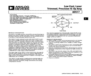
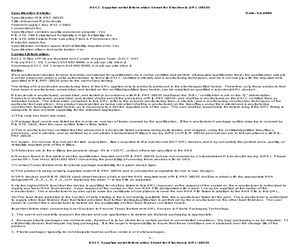
ION OFFSET NULL 1 7 tVs -IN 2 6 OUTPUT +IN 3 5 WNC 4 Vs TOP VIEW The circuit is packaged in a hermetically sealed TO-99 metal can, and is available in three performance versions (J, K, and L) specified over the commercial 0 to +70C range; and one version (AD517S) specified over the extended temperature range, -55C to +125C. PRODUCT HIGHLIGHTS 1. Offset voltage is 100% tested and guaranteed on all models. 2. The AD5S17 exhibits extremely low input bias currents without sacrificing CMRR (over 100dB) or offset voltage stability. 3. The AD517 inputs are protected (to +Vg), preventing offset voltage and bias current degradation due to reverse break- down of the input transistors. 4. Internal compensation is provided, eliminating the need for additional components (often required by high accuracy IC op amps). 5. The AD517 can directly replace 725, 108, and AD510 am- plifiers. In addition, it can replace 741-type amplifiers if the offset-nulling potentiometer is removed. 6. Thermally-balanced layout ins
 6 Pages, 181 KB, Scan
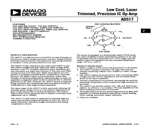
OFFSET NULL 8 1 7 +Vs5 -IN 2 6 OUTPUT +IN 3 5 NC 4 a Vs TOP VIEW The circuit is packaged in a hermetically sealed TO-99 metal can, and is available in three performance versions (J, K, and L) specified over the commercial 0 to +70C range; and one version (AD517S) specified over the extended temperature range, -55C to +125C. PRODUCT HIGHLIGHTS 1. Offset voltage is 100% tested and guaranteed on all models. 2. The AD517 exhibits extremely low input bias currents without sacrificing CMRR (over 100dB) or offset voltage stability. 3. The AD517 inputs are protected (to tVg), preventing offset voltage and bias current degradation due to reverse break- down of the input transistors. 4. Internal compensation is provided, eliminating the need for additional components (often required by high accuracy IC op amps). 5. The AD517 can directly replace 725, 108, and AD510 am- plifiers. In addition, it can replace 741-type amplifiers if the offset-nulling potentiometer is removed. 6. Thermally-balanced layout insu
 6 Pages, 309 KB, Scan
T QML DATABOOK PT QML DATABOOK PT QML DATABOOK PT QML DATABOOK PT AD652SE/883B AD664SD-BIP/883B AD632TH/883B AD538SD/883B AD2S80ASE/883B ANALOG (4) ANALOG (4) ANALOG (4) ANALOG (4) ANALOG (4) QML DATABOOK PT QML DATABOOK PT QML DATABOOK PT QML DATABOOK PT AD517SH/883B AD521SD/883B AD524SE/883B AD532SE/883B CONVERTER, V-F AND F-V D/A CONVERTER, 12-BIT, QUAD MULTIPLIER, 4-QUADRANT MULTLTIPLIER RESOLVER-TO-DIGITAL CONVERTER, 4 ARC MINUTE ACCURACY AND 10 TO 16 BITS RESOL. OP AMP, PRECISION INSTRUMENTATION AMPLIFIER INSTRUMENTATION AMPLIFIER, PRECISION ANALOG MULTIPLIER, 4-QUADRANT QML DATABOOK PT QML DATABOOK PT QML DATABOOK PT QML DATABOOK PT AD534SE/883B AD534TE/883B AD582SH/883B AD537SH/883B ANALOG MULTIPLIER, 4-QUADRANT ANALOG MULTIPLIER, 4-QUADRANT SAMPLE AND HOLD AMPLIFIER VOLT.-TO-FREQUENCY CONVERTER ANALOG (4) ANALOG (4) ANALOG (4) ANALOG (4) QML DATABOOK PT QML DATABOOK PT QML DATABOOK PT QML DATABOOK PT QML DATABOOK PT AD669SQ/883B AD548SH/883B AD549SH/883B AD561TD/883B AD566ASD/883B D/A CO
 581 Pages, 2296 KB, Original
OFFSET NULL 8 1 7 +Vs5 -IN 2 6 OUTPUT +IN 3 5 NC 4 a Vs TOP VIEW The circuit is packaged in a hermetically sealed TO-99 metal can, and is available in three performance versions (J, K, and L) specified over the commercial 0 to +70C range; and one version (AD517S) specified over the extended temperature range, -55C to +125C. PRODUCT HIGHLIGHTS 1. Offset voltage is 100% tested and guaranteed on all models. 2. The AD517 exhibits extremely low input bias currents without sacrificing CMRR (over 100dB) or offset voltage stability. 3. The AD517 inputs are protected (to tVg), preventing offset voltage and bias current degradation due to reverse break- down of the input transistors. 4. Internal compensation is provided, eliminating the need for additional components (often required by high accuracy IC op amps). 5. The AD517 can directly replace 725, 108, and AD510 am- plifiers. In addition, it can replace 741-type amplifiers if the offset-nulling potentiometer is removed. 6. Thermally-balanced layout insu
 6 Pages, 309 KB, Scan


