d for 48 hours at +150C, temperature cycled from -65C to +200C, and subjected to a high G shock test to assure reliability and long-term stability. OPERATIONAL AMPLIFIERS 278SPECIFICATIONS (typical @ +25C and +15V de unless otherwise noted) 1 MODEL AD517J AD517K AD517L AD517S OPEN LOOP GAIN 6. * Vo = 10V, Ry > 2k2 10 min Tein to Tax 500,000 min . * 250,000 OUTPUT CHARACTERISTICS . . Voltage @ Ry 2 2kQ, Thin tO Trax +10V min * : : Load Capacitance 1000pF * : : Output Current 10mA min * : . Short Circuit Current 25mA * FREQUENCY RESPONSE . . Unity Gain, Small Signal 250kHz * : Full Power Response 1.5kHz * * : Slew Rate, Unity Gain 0.10V/us * * INPUT OFFSET VOLTAGE as Initial Offset, Rg < 10k 150uV max 50nV max 25uV max vs. Temp., Tiyan to Trax 3.0uUV/C max 1.0uV/ C max 0.5uV/ C max ** vs. Supply 25uV/V max 10uV/V max ** ** (Trin tO Trax) 40uV/V max 15uV/V max ** 20uV/V max INPUT OFFSET CURRENT Initial 1inA max 0.75nA max 0.25nA max ** Tmin tO Tynax 1.5nA max 1.25nA max 0.4nA max 2nA max INPUT BIAS
 6 Pages, 428 KB, Scan
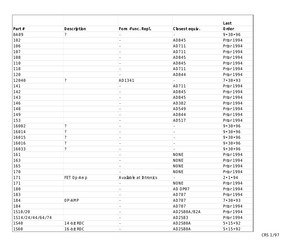
Prior 1994 4*1*96 CRS 1/97 AD395TD AD396SD AD396SD/883B AD396TD AD396TD/883B AD420AN AD420AR AD501 AD501 AD5010/6020 AD502 AD503JH AD503KH AD504 AD505 AD506JH AD506SH/883B AD507 AD508 AD509 AD510LH AD511 AD512 AD513 AD514 AD515 AD515AJH/+ AD515AKH/+ AD516 AD517KH/+ AD517LH/+ AD517SH AD518 AD520 AD5201 AD5202 AD5204 AD5205 Quad 12-bit DAC Quad DAC Quad DAC Quad DAC Quad DAC 16-bit Serial 4-20mA DAC 16-bit Serial 4-20mA DAC OP-AMP Op-Amp Op-Amp Op-Amp Amp Amp Amp Amp Amp Amp Amp Amp Amp Amp AD395JD/KD AD396JD AD396JD AD396KD AD396KD AD420AN-32 AD420AR-32 AD515A AD515AJH AD515AKH AD517KH AD517LH AD517SH/883B - AD711 None AD9000 AD711 AD548AH AD548BH OP77 AD843 AD711,AD654,AD549 AD42626 OP42 AD517 AD843 OP77EJ AD711 AD711 AD711 AD711 AD711 AD817 AD524 AD578 AD5212 AD5214 AD5215 4*1*96 9*30*96 9*30*96 9*30*96 9*30*96 10*2*95 10*2*95 Prior 1994 Prior 1994 Prior 1994 Prior 1994 9*30*96 9*30*96 9*30*96 Prior 1994 9*30*96 Prior 1994 Prior 1994 Prior 1994 Prior 1994 9*30*96 Prior 1994 Prior 19
 43 Pages, 51 KB, Original
aked for 48 hours at +150C, temperature cycled from -6 5Cto +200C, and subjected to a high G shock test to assure reliability and long-term stability. OPERATIONAL AMPLIFIERS 47SPECIFICATIONS (typical @ +25C and +15V de unless otherwise noted) MODEL AD517J AD517K AD517L AD517S' OPEN LOOP GAIN Vo = #10V, Ry > 2kQ 10 min * * * Trin tO Tmax 500,000 min * 250,000 OUTPUT CHARACTERISTICS Voltage @ Ry > 2kQ, Trin CO Tmax +10V min * * * Load Capacitance 1000pF * * * Output Current 10mA min * * * Short Circuit Current 25mA * * * FREQUENCY RESPONSE Unity Gain, Small Signal 250kHz * * * Full Power Response 1.5kHz * * * Slew Rate, Unity Gain 0.10V/us * * * INPUT OFFSET VOLTAGE Initial Offset, Rg < 10k2. 150uV max 50puV max. 25uV max ** vs. Temp., Thin tO Trax 3.0uV/C max 1.0nV/C max 0.5uV/C max ** vs. Supply 25uV/V max 10uV/V max ** ** (Trin CO Trax) 40uV/V max 15uV/V max ** 20uV/V max INPUT OFFSET CURRENT Initial 1inA max 0.75nA max 0.25nA max ** Trin CO Tax 1.5nA max 1.25nA max 0.4nA max 2nA max INPUT BIAS
 6 Pages, 452 KB, Scan
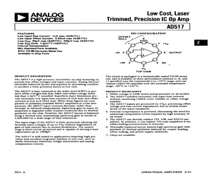
ly-balanced layout insures high open-loop gain inde- pendent of thermal gradients induced by output loading, offset nulling, and power supply variations. 7. Chips are available. OPERATIONAL AMPLIFIERS 2-51AD517 SPECIFICATIONS (a +2 anv, = = 15V de) ADS17J AD517K ADSI7L ADS517S Model . Min Typ Max Min Typ Max Min Typ Max Min Typ Max Units OPEN LOOP GAIN Vo = *10V,R, = 2k0 10 10* 10 10 vA Tenia t0 Trax, Re = 2k. 500,000 500,000 500,000 250,000 VN OUTPUT CHARACTERISTICS Voltage @ Rr = 2k2, Trin to Tux +10 +10 +10 +10 v Load Capacitance 1000 1000 1000 1000 pF Output Current 10 10 10 10 mA Short Circuit Current 25 2s 25 2s mA FREQUENCY RESPONSE Unity Gain Small Signal 250 250 250 250 kHz Full Power Response 1.5 1.5 15 1.5 kHz Slew Rate, Unity Gain 0.10 0.10 0.10 0.10 Vips INPUT OFFSET VOLTAGE Initial Offset 150 75 50 vi) pv Input Offset vs. Temp. 3.0 18 13 18 aVPC Input Offset vs. Supply 25 10 10 10 py Train t0 Tmax 40 15 15 20 pvv INPUT BIAS CURRENT Initial 5 2 1.0 2.0 nA Train ( Tmax 8 3.5 LS 10 nA
 6 Pages, 309 KB, Scan
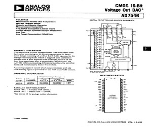
g input terminal of Al or A2 in amps Vrert - VREF~ 1LSB = ON volts N is determined by the required system resolution up to N = 16, R = R segment, typically 2kQ Low bias current op amps, BIFET or Super-Beta types, should be used such as the AD542K, AD544K, AD517K, TLO71, TLO81. Table III lists some important parameters against various op amps. Note that the AD7546 output settling time is dependent upon the op amps used. The figures in column two give the additional offset voltage contribution to nonline- arity of Al and A2. VOL. |, 9-244 DIGITAL-TO-ANALOG CONVERTERS Maximum Settling Time (us) Additional to +1/2LSB Al, A2 Nonlinearity 14 Bits 16 Bits 2X AD5S44KH 0.01% 15 35 1 X TLO72BCP (Dual) +0.05% 5 10 2X AD517JH +0.003% 90 100 1X AD644JH (Dual AD544) +0.01% 15 35 2X LF256 +0.05% 5 10 Settling time measurements were made with a similar op amp to buffer VouT (A4 in Figure 8) Table 111, AD7546 Performance vs. A1, A2 . DATA LOADING AND DEGLITCH SWITCH The AD7546 timing specifications are included o
 8 Pages, 618 KB, Scan


